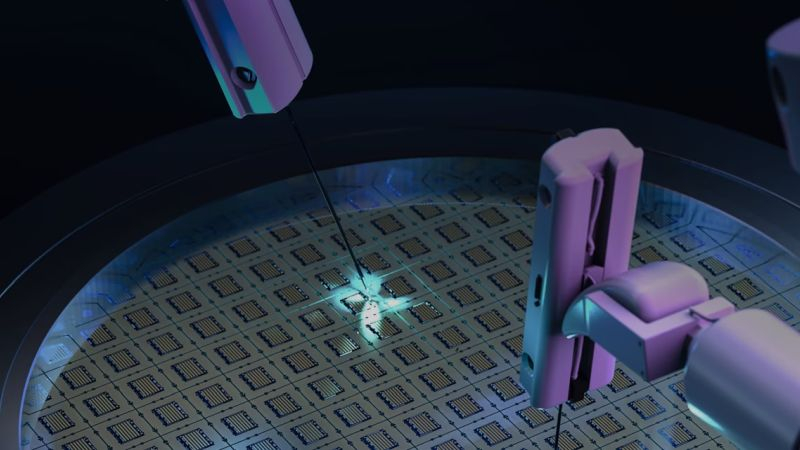
Samsung Unveils Chip Production Plans
South Korean tech giant, Samsung Electronics, intends to introduce 1.4nm lithographic standards by 2027 and a power substrate on the back side of the silicon wafer as part of the 2nm process technology. Samsung harnessed 3nm production combined with the application of Gate-All-Around (GAA) transistor structure back in mid-2022, surpassing all competitors, but it didn’t bring significant success among its customers.
Plan Revealed in Recent Company Briefing
This development emerged following a briefing by Samsung representatives at a recent industry event, as reported by Bloomberg and Reuters. The company stressed to its clients that it can simultaneously supply them with High Bandwidth Memory (HBM) accelerators, manufacture chips, and handle their subsequent packaging. Such a combination of expertise allows Samsung to significantly reduce the production cycle time by 20%.
Forecasted Growth in Semiconductor Market
Samsung predicts that by 2028, the semiconductor market will surge to $778 billion, largely due to an increase in the use of computation accelerators in artificial intelligence systems. The company is banking on a fivefold increase in the number of clients ordering the manufacture of such products by this point and aims to see 9 times higher associated revenue. Echoing the views of OpenAI founder, Sam Altman, Samsung sees the academia’s need for production capacities to manufacture computation accelerators. Altman added that to meet demand, dozens of new chip-making facilities need to be built.
Samsung’s Focus on GAA Transistors and Future Developments
Samsung argues that GAA transistors will play an increasingly significant role in the manufacture of complex chips using cutting-edge technologies. The company is set to start mass production of 2nd generation 3nm chips in the latter half of this year. The GAA transistor structure will be used in Samsung’s 2nm process as well. Furthermore, the company plans to introduce a power source rear-side silicon wafer within the second generation of its 2nm process technology. By 2027, Samsung plans to have mastered the production of chips using 1.4nm technology. Market research firm, TrendForce, highlighted that Samsung’s share in the chip contract manufacturing market has steadily declined from 11.3% to 11% in the first quarter of this year. Industry leader TSMC has seen an increment in its share from 61.2% to 61.7%.