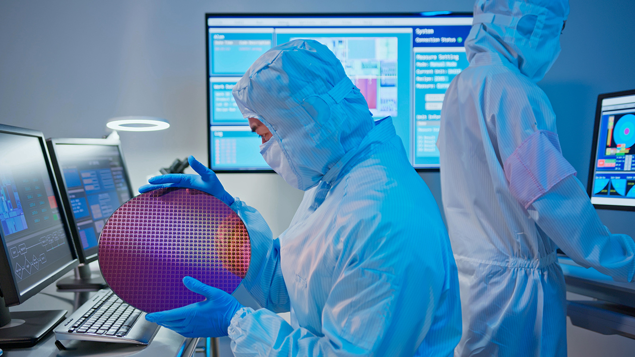
Advancements in the field of computational accelerators have been hindered by limitations in TSMC’s chip testing and packaging capacities in the CoWoS technology. To address these constrains, TSMC is reportedly considering constructing a testing facility in Japan, according to Reuters.
As previously reported, TSMC already operates two facilities in Japan that handle silicon wafers using mature lithography. Their research center focused on the utilization of various innovative materials and chip packaging methods primarily serves TSMC’s interests rather than those of its Japanese partners who supply materials and technological equipment.
As chip-makers in Japan begin to adopt advanced lithography for their products, TSMC’s additional CoWoS packaging and testing facility could provide significant benefits. In particular, Japanese consortium Rapidus, which plans to launch the production of advanced 2-nm chips in Japan by 2027, could be a major beneficiary of this initiative. However, no firm details are available yet regarding the schedule and budget for the construction of the new TSMC facility. At present, TSMC’s significant clients requiring CoWoS chip packaging services are predominantly US companies, as noted by TrendForce experts.
It’s worth noting that Intel and Samsung also plan to leverage the expertise of Japanese equipment manufacturers and material suppliers. Intel is considering constructing a dedicated research center in Japan, while Samsung has already reached an agreement with local partners to achieve the same. It should be remembered that TSMC already operates such a research center in Japan.