Taiwan Semiconductor Manufacturing Company (TSMC) senior vice president, Kevin Zhang re-affirmed in late April that he believes it’s not feasible to implement ASML’s High-Numeric Aperture (High-NA) lithography equipment for chip production using the A16 technology set to be operational in the second half of 2026. This week, he reiterated his stance during a technology symposium held in the Netherlands, citing the equipment as being too expensive.
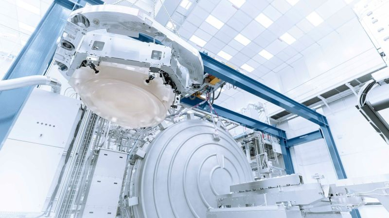
Zhang expressed admiration for the capabilities of High-NA EUV equipment, but its high price tag proved unattractive. The next-generation ASML equipment that was highlighted during the discussion can produce semiconductor elements as thin as 8nm, a 1.7 times improvement over previous generation lithographic scanners. However, this 70% improvement comes at a significant cost with each unit retailing at $380 million, compared to approximately $216 million for regular scanners.
It’s worth noting that ASML is currently testing one of such scanners for High-NA EUV. A second unit has been installed at Intel’s research center in Oregon, and a third is allocated for Imec, a Belgian company partnering with the Japanese consortium, Rapidus. Rapidus plans to commence production of 2nm products in Japan by 2027. Intel aims to experiment with High-NA EUV in its 18A technology but will likely only implement it in commercial production by the time it launches the Intel 14A technology in 2027. Intel has reportedly purchased the full supply of ASML’s next-generation lithographic scanners for this year to prepare adequately.
Zhang, on behalf of TSMC, Taiwan’s dominant contract chip manufacturer, maintained optimism about maximizing their current equipment’s capabilities. He explained that TSMC facilities planning to utilize the A16 process could be retrofitted to accommodate High-NA EUV equipment. However, the actual timing of when such equipment would be required remains uncertain. According to Zhang, TSMC’s decision on the implementation timeline will balance the technical characteristics of the chips produced and the economic factors involved. He added that the entire industry is grappling with rising costs in chip factory construction, equipping, and operation.