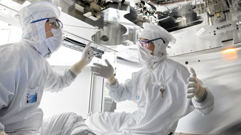
Netherlands-based ASML remains the principal supplier of lithographic scanners essential for the manufacturing of semiconductor components. It has recently begun shipping its advanced High-NA EUV equipment that will be installed in a newly established laboratory in collaboration with Belgian-based Imec for company clientele.
High-Value Laboratory Equipment for Chip Makers
A new ASML laboratory, providing semiconductor component manufacturers with early access to a high numerical aperture (High-NA) equipment capabilities, is set to open in Veldhoven, the Netherlands, after several years of construction. Each high-NA scanner costs up to 350 million euros making it realistically affordable for hands-on experimentation by a select few companies, such as Intel since December of the previous year. However, accessing such equipment in ASML’s laboratory is considerably simpler.
Advanced Technology Adoption on the Rise
This high numerical aperture equipment boosts the resolution capabilities of lithographic scanners by 60%. Intel plans to incorporate this technology in their 14A chip production, while TSMC, in contrast, is not in a hurry to adopt it, choosing to remain content with existing solutions for its A16 process technology. ASML emphasized this week that its customers will begin using their High-NA EUV equipment in commercial chip production by either 2025 or 2026.


