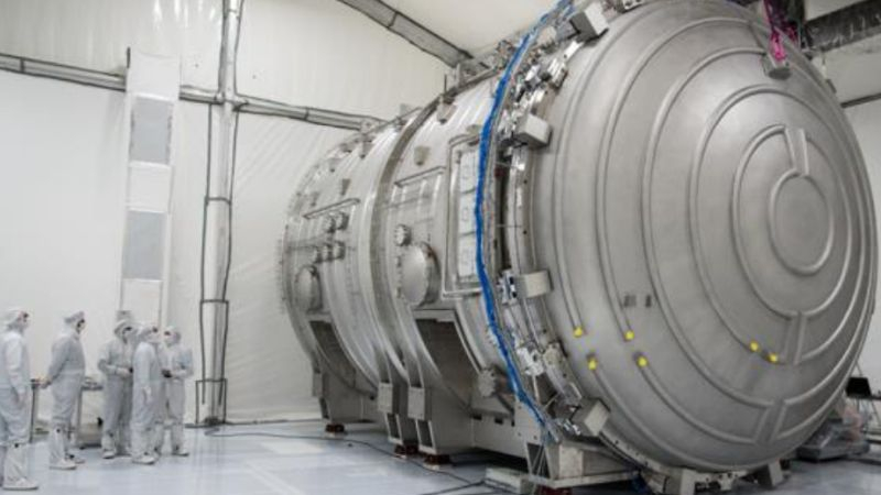
Intel is set to utilise the first photolithography scanner with a high numerical aperture from ASML in its Oregon research center for Intel 18A technology experiments. ASML, however, suggests that these scanners won’t see mass production until 2026-2027. The equipment was delivered to Intel as early as December last year but is not expected for use in volume production of Intel 18A chips.
This week, as reported by Reuters, Dutch company ASML invited press representatives to its facility to show samples of its High-NA equipment and discuss future applications.
ASML and analysts diverge on projections regarding the reasonable use of High-NA tools in mass chip production. Semianalysis experts suggest that the economically viable use of these lithographic scanners wouldn’t be until at least 2030. ASML refutes this, asserting that the move to the new generation of scanners will result in economic gains much earlier, starting in 2026 or 2027.
Samsung and TSMC have already shown interest in ASML’s equipment. However, TSMC’s management recently signaled that the economic feasibility will significantly affect their technology adoption timeline. Notably, TSMC won’t force its customers to shift to the new equipment if it’s unfit for their processes. This reluctance indicates that TSMC isn’t in a hurry to employ high-NA lithographic scanners currently.
ASML announced this week that its High-NA lithographic systems weigh 150 tons and occupy 250 containers when disassembled. Setting up such a scanner for operation requires the effort of 250 engineers over six months. ASML currently has between 10 to 20 orders from clients for such scanners, including memory manufacturers like Micron and SK hynix. By 2028, ASML plans to produce up to 20 such systems annually. Chip manufacturers can use this new equipment to reduce semiconductor element sizes by 40%, thus tripling transistor density. Each system costs around $380 million. Multiple units of this equipment are expected to be shipped to clients this year.


