New Litographical Scanners Expected in the Next Decade
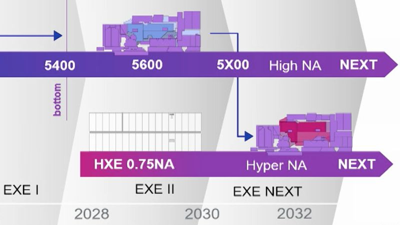
ASML, a leader in the lithography scanner market, hinted back in May at the potential for systems capable of handling ultra-high numerical aperture figures by the start of the next decade – 0.75(Hyper-NA EUV). Imec representatives suggest that lithography will still be reliant on lasers and silicon in the next decade.
Imec Forecasts Future of High-NA EUV
Kurt Ronse, Director of Advanced Exposure Programmes at Imec, shared his insights with EE Times. The Belgian company has been assisting ASML for over 30 years in the development of new technologies for lithographic scanners, and he rightly anticipates their future development. Currently, as manufacturers move towards high numerical aperture flaggers (0.55 High-NA EUV), equipment makers face several challenges.
One challenge with a numerical aperture of this magnitude is the emergence of light polarization, reducing the contrast of the projected image on the silicon plate. Polarization filters can address the issue, but they increase energy consumption and product costs. According to Imec, transitioning to Hyper-NA EUV will require new photoresist materials, as even with a numerical aperture of 0.55, their layer thickness decreases, thus impairing the precision of subsequent chemical etching.
TSMC and Intel’s Adoption of High-NA EUV
Ronse suggests TSMC is not in a rush to move to High-NA EUV due to its vast experience with multiple photomasks. Intel lacks similar experience and hence prefers transitioning to costly equipment with better resolution. Dual templating would require more precise photomask positioning, an area where Intel lacks expertise. According to Imec, TSMC might consider transition to High-NA EUV towards the end of this decade.
In general, this equipment will be employed in chip production using lithographic standards thinner than 2 nm – up to 7 angstrom. After this, lithographic scanners with ultra-high numerical aperture (Hyper-NA EUV) usage will come in. The shift will eliminate the need for double templating, which elevates tooling costs and extends the production cycle, thereby increasing product costs.
Alternatives to High-NA EUV
Imec researchers have considered several alternatives to ultra-high numeric aperture lithographic equipment. One is the technology of nano-printing transistors, but it lags significantly behind even the High-NA EUV scanners regarding productivity. Another considered alternative was the use of multiple-directed electron streams to form the required pattern on the silicon plate, but the sole manufacturer of suitable equipment declared bankruptcy.
Employing new materials in place of silicon also poses difficulties, Imec explains. There exist materials with higher electron mobility, but applying them onto a plate which remains silicon-based is a complex process. Deploying equipment for applying new materials coincide with innovative chemicals, and relative experiments are ongoing, but they are far from mass usage.