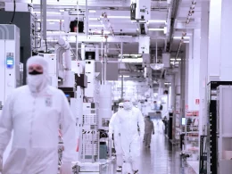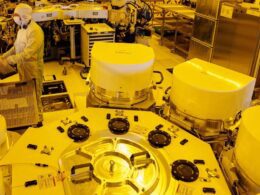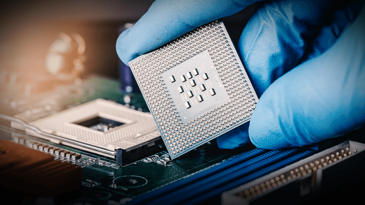
Artificial intelligence (AI) has found its purpose not only in the development of chips and their corresponding software but also in the creation of technological toolkits for their production. At least this is the case for Nvidia and Synopsys whose cooperative work has resulted in the significantly expedited process of photomask development and incorporation of corrective measures in technical processes during chip production via optical lithography.
A press release on Nvidia’s website clarifies that the corporation, in collaboration with Synopsys – a software developer for chip design and technological toolkit creation, employed artificial intelligence to optimize the software platform cuLitho. The said platform uses GPU computing potential for the optimization of the photomask design process in chip production.
Firstly, the transfer of these key computations from central processors to graphics accelerates photomask development, an increasingly important aspect in the production of modern chips due to the ongoing adoption of finer lithography norms. With central processors, these computations might take 30 million hours or longer. However, a system with 350 Nvidia H100 accelerators can replace a data processing center with 40,000 central processors. This substitution not only mitigates the amount of space required for equipment but also reduces energy consumption.
TSMC, the largest contract chip manufacturer, is incorporating Nvidia’s cuLitho solutions into its technical processes that were introduced last year. Synopsys is also transitioning the Proteus software used for optical correction calculation in photomask design to the Nvidia cuLitho platform. This shift has led to a doubling of the process speed in comparison to the exclusive use of central processor computational resources. These solutions will gain support from Nvidia’s Blackwell family of accelerators in the future.