Taiwan Semiconductor Manufacturing Company (TSMC) has unveiled an aggressive roadmap for its nano-manufacturing processes. Representatives revealed last week that serial production of the N3P chips would commence by the end of the year. Leading tech website AnandTech consolidated all information about the company’s immediate plans. Four new processes are set to be incorporated in 2025 and 2026.
The N3X and N2 processes are slated for 2025, with focus targeted towards the second half of the year. These two processes, in some respect, will vie for TSMC client preferences. N3X is expected to downsize power consumption by 7% compared to N3P, due to begin in the latter half of this year. Despite constant transistor density, the N3X switching speed will grow by 5% at 1.2V voltage, while density will increase by 1.1 times keeping the clock frequency constant.
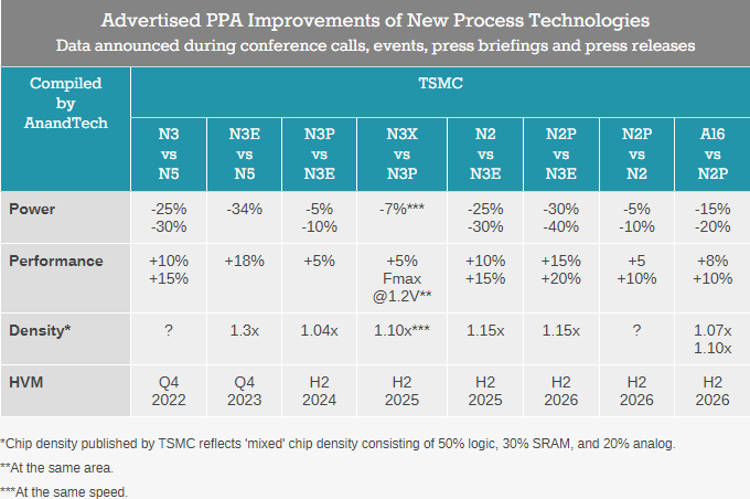
The N2 process promises a 25-30% reduction in power consumption relative to the N3E, mastered from Q4 last year. Concomitantly, transistor switching speed will go up by 10-15%, along with a 1.15 times increase in transistor density. The N2P process, planned for the second half of 2026, promises the same density, but energy consumption will reduce further by 30-40% while transistor switching speed will hike by 15–20%. Hence, a direct comparison of N2 and N2P doesn’t render a notable distinction in energy consumption (5-10%) and speed (5–10%), while transistor density remains unchanged.
As part of the N2 process, TSMC will introduce nano-sheet and gate-all-around (GAA) transistor structures for the first time. This is expected to significantly enhance performance, reduce power consumption and increase transistor density. The N3X process might outdo N2 in performance, especially at higher voltages, primarily due to unchanged transistor structures (FinFET), helping to reduce defect levels.
TSMC plans to master the N2P and A16 processes in 2026. A16 will focus more on increasing base N2 performance and offer 1.6nm technology capabilities combined with reverse-side silicon plate power supply. N2P could either offer a 5-10% reduction in energy consumption or simultaneously increase performance at identical energy consumption rates in comparison with basic N2.
The A16 process promises a 20% reduction in energy consumption from N2P, or a performance boost by 10% at the same energy consumption levels. The A16 transistor density will allow a 10% increase from N2P. Power supply from the reverse side of the silicon plate for high-performance-oriented chips makes the A16 process pretty costly to manufacture.