Intel’s High-NA EUV Equipment Bet: A Potential Risky Affair
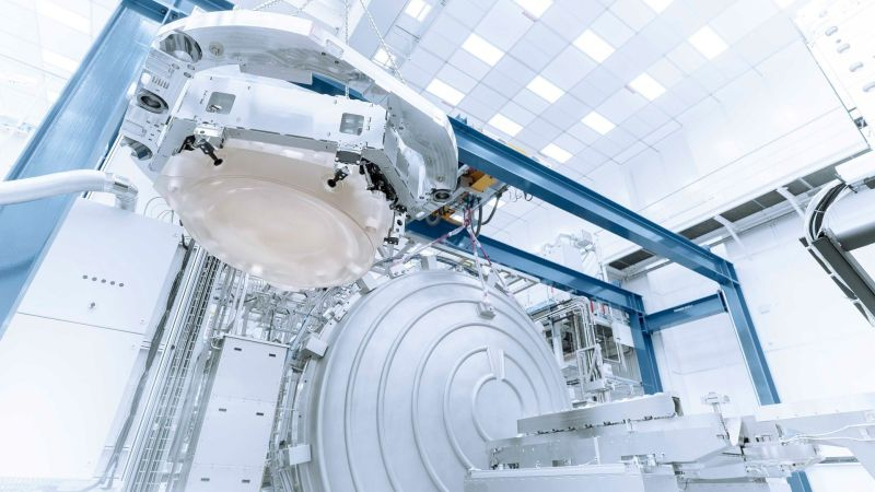
This month, it emerged that Intel might have procured all the latest generation ASML lithographic scanners (High-NA EUV) available this year. Contrarily, TSMC insists it can deploy the A16 technology without such expensive equipment. Experts warn Intel could face substantial losses if this strategy backfires.
A High Stakes Bet
In pursuit of chip production cost reduction to levels unattainable by competitors, Intel CEO, Patrick Gelsinger, is keen on rapid adoption of High-NA EUV scanners. The concern is that each ASML lithographic scanner with a high numerical aperture (High-NA) costs about $380 million, nearly twice the amount of a regular EUV scanner.
Even if Intel rolls out High-NA EUV technology gradually, layer by layer, it will require a considerable amount of this costly equipment. According to ITRI analysts surveyed by TrendForce, this has set up the company for a potential financial pitfall.
A Calculated Approach: A Potential Warning
The skeptics argue that TSMC’s cautious approach to High-NA EUV adoption should serve as a warning for other foundry service enterprises. Despite being market leaders with a sizable customer base, TSMC appears to understand that rushing to adopt this new class of equipment isn’t necessary. The technological advantages the scanners offer aren’t compelling enough to justify their substantial acquisition costs.
Despite this, when the need arises unquestionably, TSMC will undoubtedly transition to High-NA lithographic scanners. Until then, the Taiwanese manufacturer prefers to hold back.
Intel’s Potentially Tricky Path
ITRI experts believe Intel is currently undervaluing the importance of chip layout and packaging technologies. They feel the company is placing a calculated bet on lithography. However, Intel’s leadership has made its decision. It remains to be seen how this strategy impacts the business of the processor giant in dire need of serious reforms and substantial capital investments.


